OSA Science & Applications of Nanolasers Incubator: Day 1
Shuai Sun, George Washington University
Day 1 of the Science & Applications of Nanolasers Incubator brought something new for OSA Incubators. Due to construction at OSA headquarters, this program is being held at the Science and Engineering Hall (SEH) of George Washington University in Washington, D.C. The topic of this meeting, the Nanolaser, has become one of the hottest topics in the optical field. The semiconductor lasers with wavelength scale or below has been applied onto many real world applications, such as photonic crystals, nanowires, metal claddings, etc. The size scaling and the energy efficiency scaling nowadays becomes the major targets in this research field.
The goal of this Incubator is to forge connections between the diverse communities working on different approaches to nanolasers in order to identify fundamental goals and limits for nanolaser research, identify potential applications for nanolasers and identify a roadmap for nanolaser research that can bring the science closer to commercialization.
To kick off the Incubator, the GW Associate Dean of Research and Graduate Studies Dr. Can Korman and the OSA Foundation Executive Director Chad Stark welcomed the group. Rupert Oulton, from the Imperial College London and one of the hosts of this program, gave a talk about the motivations for small lasers from the first laser back to 1960 to the present plasmonic lasers. He expanded it to the recent problems and thoughts for recent sub-wavelength lasers. Then, the topic is passed to Renmin Ma from Peking University, another host, to discuss the localization of light in the frequency, time and space domain. He showed a few experiment results between photonic lasers and plasmonic lasers among sizes, volumes, threshold powers and areas. Finally, Volker Sorger, the third host of this meeting and the reason this meeting was generously held at George Washington University where he is an assistant professor provided an overview of the rest of the program and introduced the first keynote speaker.
Ming Wu from UC Berkeley, introduced the basic semiconductor and metallic cavities and then compared different kind of optical emitters from traditional laser to VCSEL, photonic crystals, nano lasers, plasmonic lasers and then nano LEDs which are ideally make as low quality factor devices with rather small footprints. Dr. Wu explained that the main driving force of the on-chip interconnect links in the future is the energy efficiency, and he also predicted that the ideal goal of the communication sensitivity is about 100 photons/bit (=100 aJ/bit), which is two orders of magnitude lower than we currently have in our recent interconnects. Then he provided a novel structure that has a nano LED with metal antennas on each side, which benefits in no threshold, higher bandwidth frequency and easier emission. In the end, Dr. Wu concluded that with fundamental trade-offs between energy efficiency and enhancement in mind, 1000 times of enhancement with 50% efficiency is able to be achieved.
During the Optical Confinement & Feedback in Nanolasers session, Mikhail Noginov, Norfolk State University, gave a talk about plasmonic lasers in strong coupling environments and stated that the dye molecules with plasmons are able to create strong couplings, and large normal mode splitting is easy to achieve experimentally. After that, Dr. Cun-Zheng Ning, Arizona State University, spoke about the necessity of having smaller and more efficient lasers. He predicted that by the year 2020, 20 MW is needed only to power the optical interconnect links of a super computer. And for the nanophotonic integration, the major challenge is size mismatches with much larger laser footprint. Then, he showed the Semiconductor-Metal Core-Shell nanolaser from his group which is the first electrical injection sub half-wavelength laser with 460nm critical length. Si-Hui Athena Pan from University of California discussed the recent research results from her group in the topic of coherence and dynamics of metal-clad nanolasers. She explained and compared the optical and electrical pumped cavities with coaxial cavity and showed their recent metal-clad nanolaser design. By using the g2 measurement, a unity-β laser has been proven with dynamical hysteresis. Before lunch, Dr. Mercedeh Khajavikhan from University of Central Florida, first introduced a few recent coupled PT micro-cavities and then showed the basic theory and structure of their PT-symmetric micro ring design. The result shows there is no power loss in the PT-symmetric laser and it direst almost four times of power. She concluded that non-Hermitian exceptional point is able to provide a new paradigm in laser mode management.
After lunch the Nano-Cavities and the Purcell Effect session kicked off with Maiken Mikkelsen, Duke University. She gave a talk on the nano-cavities and Purcell effect especially focus on sub-10 nm gaps between materials. She first explained different approaches to reach sub-10 nm gap and he pointed out that nano scale patch antennas which is the commonly used structure in the field is able to provide over 100 times of electrical field enhancement. In her recent design, gaps and cube sizes are the two controllable nodes in order to achieve the tunability of plasmonic resonance. Dr. Sorger then spoke about the Purcell effect in Hybrid Plasmonic Nanowires and cavity scaling laws. He started with the reason why we need nano scaling by analyzing the cavity scaling, optoelectronic device scaling, output coupling and the laser performance comparison. Ritesh Agarwal, University of Pennsylvania, wrapped up the session by starting with a question – “How does light interact with matter?” He then talked about single nanowire lasers and utilizing nanowire as a FP cavity. He used the exciton-Polaritons to generate strong Light-Matter-Interaction.
After another break, where the discussions continued, the Incubator turned to Nano-Laser Arrays. Vladamir Shalalev of Purdue University talked about the wavelength-tunable gold nanorod spacers. He introduced the plasmonic lasers and random lasers that his group worked on from 1D nanoparticle to 2D metal metasurface and finally 3D metal netamaterial. Also, he compared the basic lasing properties between HMM and EMM by looking into laser mechanism and basic functions. Boubacar Kante, UC San Diego continued with his talk on bound state in the Continuum Nanophotonic Cavities and Lasers. He introduced the basic principles, functions of symmetries of multipoles and then showed the first BIC laser with inspiring results. The last speaker for the day, Danqing Wang from North Western University showed the plasmonic nanocavity array design which has band-edge state with near-zero group velocity. The laser action in strongly coupled plasmonic nanocavity arrays have the benefit such as directionality, tunability and room temperature operations. On the tunability side, the plamonic nanocavity array is able to provide real-time tuning and on the side, it is able to provide multi-frequency.
Stay tuned for more from day 2 of the OSA Science & Applications of Nanolasers Incubator!
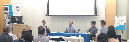
Hosts Renmin Ma, Rupert Oulton and Volker Sorger join keynote Ming Wu, UC Berkeley to discuss the motivations for small light sources.