Solutions and Approaches to Break Opto-electronic Device Limitations
Ke Liu
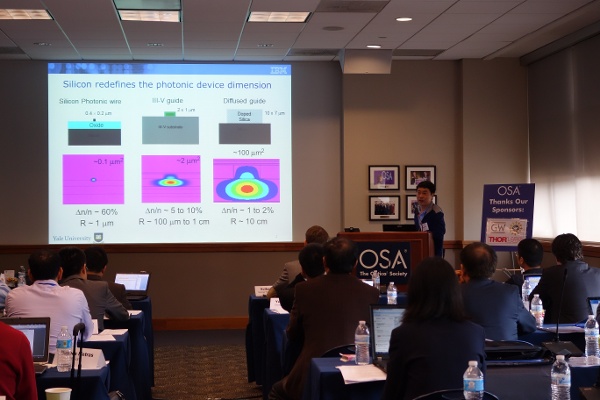
There is a Chinese saying, “even a clever housewife cannot cook a meal without rice.” Material science is always the mostly elementary research field, since any novel opto-electronic components depend on new properties of materials. Conventional semiconductor materials, i.e. Silicon and III-V, show fundamental limit to some photonic devices. The possible roles of emerging two-dimensional (2D) materials such as graphene, transition metal dichalcogenides, and black phosphorus (BP) in photonic integrated circuits are thus explored for optical communications. These emerging 2D materials have tunable band-gap by material composition and layer numbers, and they may cover the entire infrared wavelength range. In addition, its layered nature allows for the isolation of single and few-layer materials which can be integrated seamlessly with any photonic platform. What kinds of emerging materials may be applied in nanophotonics? The talk was presented by Fengnian Xia. Graphene, a kind of 2D material, is pure carbon in the form of a very thin, nearly transparent sheet, one atom thick. Due to its interaction with light from visible to terahertz range, as well as effective tuning using E-field, high-speed graphene photodetectors and modulators were introduced. Also, taking advantage of graphene plasmonic, light-matter interactions is further enhanced, such as plasmon resonance in graphene superlattice. In the end Dr. Xia expected an on-chip optical interconnect system based on these 2D materials, including Mx2/BP as light emitter, graphene modulator and detector, graphene based electronics, while all these devices may be integrated on a Si or Silicon nitride platform.
To surpass the classical diffraction and speed-limitations, thanks to plasmonic, a bridge between photonics and nanoelectronics, presented by Volker J. Sorger, an emerging technology relies on the propagation of electromagnetic waves known as surface plasmon polaritons (SPPs) along a metal-dielectric interface. It leads to strong light-matter interaction, allowing for the deployment of optical structures with sub-wavelength dimensions, breaking the size barriers of traditional diffraction-limited optics. During his talk, Dr. Sorger described what role plasmonics can play in future device technologies and how it can complement electronics and conventional photonics, such as Lambda-size metal-oxide–semiconductor based hybrid plasmonic modulators, plasmon nanowire lasers at a deep sub-wavelength scale, etc. Plasmonics has been viewed by many researchers as a natural next generation technology platform to deliver enhanced devices performance. While significant progress has been made on a device level, this field is challenged by fundamental physics (i.e. optical losses), and potentially platform integration with existing device and PIC technologies.
A couple of more interesting topics related to photonic crystals, electrical & optical interconnect, and hybrid integration were presented in the afternoon at the incubator meeting. Although quite a few technology breakthroughs have been made so far, we are still facing arduous tasks to break the classic limitations completely. More expectation to come on the future research efforts for the aforementioned new fields and materials, as well as theoretical and experimental issues. While we cannot cover everything here, stay tuned for one more final update tomorrow, then, following the Incubator the hosts will be sharing more through an article in OPN. You can also follow this community on the Nanophotonics Technical Group website.
***
We have some photos from the event!

Thomas Koch, University of Arizona, USA

Fengnain Xia, Yale University, USA - one of the hosts.

Volker Sorger, George Washington University, USA - one of the hosts.
