About
26 September 2019
New Chip Poised to Enable Hand-Held Microwave Imaging
Researchers shrink bulky imaging systems down to millimeter sized chip that could be used to see through walls or detect tumors
WASHINGTON — Researchers have developed a new microwave imager chip that could one day enable low-cost handheld microwave imagers, or cameras. Because microwaves can travel through certain opaque objects, the new imagers could be useful for imaging through walls or detecting tumors through tissue in the body.
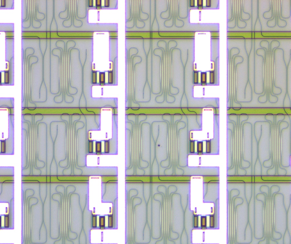
Caption: Researchers fabricated a nanophotonic microwave imager chip. It contains over 1,000 photonic devices, some of which are seen in this close-up.
Credit: Farshid Ashtiani, Electronic-Photonic Microsystems lab, University of Pennsylvania
In Optica, The Optical Society's (OSA) journal for high-impact research, the researchers describe how they used a standard semiconductor fabrication process to make a microwave imager chip containing more than 1,000 photonic components. The square chip measures just over 2 millimeters on each side, making it about half the width of a pencil eraser.
“Today’s practical microwave imagers are bench-top systems that are bulky and expensive,” said research team leader Firooz Aflatouni from the University of Pennsylvania, USA. “Our new near-field imager uses optical, rather than electronic, devices to process the microwave signal. This enabled us to make a chip-based imager similar to the optical camera chips in many smartphones.”
Hand-held near-field microwave imagers would be useful for many applications including high-resolution brain imaging and monitoring heart motion and breathing. Miniaturization of microwave imagers would also benefit applications such as tracking objects in radar systems and low-power, high-speed communication links.
Optical processing used to create microwave images
Optical cameras like the ones in smartphones use a lens to form an image on the camera’s image sensor. The new near-field imager uses four antennas to receive microwave signals reflected from an object. These microwave signals are then encoded into an optical signal and are optically processed — emulating a microwave lens — to form an image.
The chip-based imager includes more than 1,000 photonic components such as waveguides, directional couplers, photodiodes and ring modulators. One of the essential components is the optical delay element network used for signal processing, which consists of more than 280 delay cells.
“This system is significantly smaller and more efficient than its electronic equivalent because the delay cells are more than 10 times smaller and more than 10 times more efficient,” said Farshid Ashtiani, a graduate student in Aflatouni's group and coauthor on the paper. “They can also operate with significantly shorter microwave pulses, which produces higher imaging resolution.”
Demonstrating the microwave imager
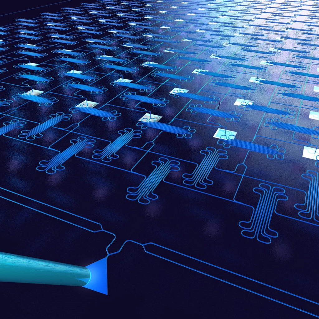
Caption: Researchers demonstrated the first nanophotonic microwave imager chip, which is significantly smaller that the equivalent all-electrical systems with a higher efficiency, and enables realization of hand-held microwave imagers for applications including through-the-wall imaging and tumor detection.
Credit: Ella Maru Studio
To demonstrate the new chip, the researchers used it to image objects with metallic surfaces, including metallic squares measuring 24 centimeters on each side and the UPenn logo. After short microwave pulses illuminated each object placed in front of the imager, the four antennas received the reflected signals, which were used to form the image of each target object.
“Our work shows that standard semiconductor fabrication techniques can be used to create robust photonic systems containing many devices,” said Aflatouni. “The tiny imager chip we demonstrated can be scaled up, enabling realization of low-cost handheld high-resolution microwave imagers.”
Now that they’ve demonstrated a chip-based microwave imager, the researchers plan to increase the number of pixels by upping the number of on-chip delay lines, using more advanced fabrication technologies and stitching together smaller images. They also want to use shorter microwave pulses to achieve higher resolution.
Paper: F. Ashtiani, A. Risi, F. Aflatouni, “Single-chip nanophotonic near-field imager: supplementary material,” Optica, 6, 10, 1255-1260 (2019).
DOI: https://doi.org/10.1364/OPTICA.6.001255
About The Optical Society
The Optical Society (OSA) is dedicated to promoting the generation, application, archiving, and dissemination of knowledge in optics and photonics worldwide. Founded in 1916, it is the leading organization for scientists, engineers, business professionals, students, and others interested in the science of light. OSA’s renowned publications, meetings, online resources, and in-person activities fuel discoveries, shape real-life applications and accelerate scientific, technical, and educational achievement.
About Optica
Optica is an open-access journal dedicated to the rapid dissemination of high-impact peer-reviewed research across the entire spectrum of optics and photonics. Published monthly by Optica Publishing Group, the Journal provides a forum for pioneering research to be swiftly accessed by the international community, whether that research is theoretical or experimental, fundamental or applied. Optica maintains a distinguished editorial board of more than 60 associate editors from around the world and is overseen by Editor-in-Chief Prem Kumar, Northwestern University, USA. For more information, visit Optica.
Media Contact
