Perspective views from Industry & Government on Nanophotonics
Ke Liu
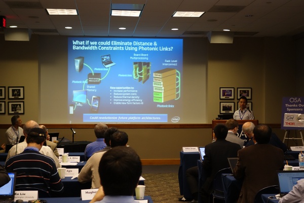
The second day of the Nanophotonic Devices Incubator, representatives from industry and government shared several perspectives on nanophotonic devices. Any novel devices have to undergo the test of the market demand. What are the current trends and future bottlenecks in high-performance photonic integrated circuits? The talks were given by Frederick Kish, Infinera Corporation, and by Jung Park, Intel Corporation, respectively. Infinera offers an outstanding representative of III-V based PIC, realizes WDM system on a photonic chip: 100Gb/s to 1Tb/s and more in the future, as well as 500Gb/s PIC-module sub-assembly for current interconnect technology. However, Dr. Kish pointed out that PIC-element density is limited by optical electrical interconnect density, optical routing, and PIC element size; and that future generation devices still require increasing power efficiency of key elements, e.g. lasers, modulators, drivers, etc. Intel offers a well-known representative of Silicon based PICs; Dr. Park showed the current bottleneck still needs a full set of devices that enable chip-scale interconnects, i.e. performance, size/density, efficiency. The other critical issue is thermal stability.
The speaker Dimitris Pavlidis, National Science Foundation, a research funding source, gave a talk on future vision for the nanophotonics mission requirement. The long-term objective is systematic understanding, control and restructuring of matter at the nanoscale for societal benefit. Specifically, 1) new theory at nanoscale, 2) investigative and transformative methods, and 3) integration of nanotechnology in application areas such as nano-manufacturing for a sustainable environment, energy conversion, nano-bio interfaces between the human body and manmade devices, nano-informatics for communications, etc.
The next panel session moved to the topic, “How to merge current nanophotonic devices solutions with emerging trends?” Rajeev J. Ram, MIT, addressed the talk on energy efficient optoelectronics. A couple of low-power consumption devices including sub-100fJ/bit transmitter, 220fJ/bit NIR receiver in native CMOS, and first bulk CMOS photonics link with 5Gb/s at 2.8 pJ/bit were demonstrated. We expect sub-14nm nodes electrical link budget to shrink to roughly 50fJ/bit, even with some challenges. However, we will see.
In terms of the military and security point of view, Luke Sweatlock, Northrop Grumman, presented a talk on merging plasmonic and nanophotnoics technology into applications for military purpose. One of the highlights is a plasmonic interconnection and signal processing system on a chip. Also, smaller optical devices, smaller camera pixels, and smaller sensors are desired to reduce the cooling burden for spacecraft modules.
**
I learned a lot from the meeting, and the interesting talks and honest discussions in all the sessions really impressed me. I am sure that you will agree with me – apart from other conventional meetings, the OSA incubator meeting has some unique features, wonderful talks, breakout group discussion, panel discussion, efficient organization as well. Hope to see you at the next OSA incubator meeting!

Jung Park, Intel - one of the hosts.
