About
29 September 2021
Researchers Integrate Optical Devices Made of Multiple Materials onto Single Chip
New method lays groundwork for practical manufacturing of chip-based optical systems for communications, imaging and more
WASHINGTON — Researchers have developed a highly accurate way to assemble multiple micron-scale optical devices extremely close together on a single chip. The new approach could one day allow high-volume manufacturing of chip-based optical systems that would enable more compact optical communications devices and advanced imagers.
“The development of electronics that are based on silicon transistors has enabled increasingly more powerful and flexible systems on a chip,” Dimitars Jevtics from the University of Strathclyde in the UK. “Optical systems on a chip, however, require integration of different materials on a single chip and, therefore, have not seen the same development in scale as silicon electronics.”
In the Optica Publishing Group journal Optical Materials Express, Jevtics and colleagues describe their new transfer printing process and demonstrate its ability to place devices made of multiple materials on a single chip, all integrated within a footprint similar in size to the devices themselves. While other methods are typically limited to a single material, this new approach provides a toolbox of materials from which future systems designers can draw.
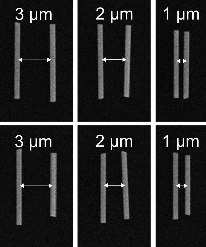
Caption: Researchers developed a new way to assemble multiple nanoscale optical devices extremely close together on a single chip. They demonstrated the transfer printing method by placing nanotubes 1 to 3 microns apart.
Credit: Dimitars Jevtics, University of Strathclyde
“On-chip optical communications, for example, will require the assembly of optical sources, channels and detectors onto sub-assemblies that can be integrated with silicon chips,” said Jevtics. “Our transfer printing process could be scaled up to integrate thousands of devices made from different materials onto a single wafer. This would enable micron-scale optical devices to be incorporated into future computer chips for high-density communications or into lab-on-a-chip bio-sensing platforms.”
A better way to pick and place
One of the biggest challenges for assembling multiple devices on a chip is trying to place them very close together without disturbing devices that are already on the chip. To accomplish this, the researchers developed a method based on reversible adhesion in which a device is picked up and released from its growth substrate and placed onto a new surface.
The new method uses a soft polymer stamp mounted on a robotic motion control stage to pick up an optical device from the substrate on which it was made. The substrate onto which it will be placed is then positioned under the suspended device and accurately aligned using a microscope. Once aligned properly, the two surfaces are brought into contact, which releases the device from the polymer stamp and deposits it onto the target surface. Advances in accurate micro-assembly robotics, nanofabrication techniques and microscopy image processing helped make this approach possible.
“By carefully designing the geometry of the stamp to match the device and controlling the stickiness of the polymer material, we can engineer whether a device will be picked up or released,” said Jevtics. “When optimized, this process does not induce any damage and can be scaled up using automation to be compatible with wafer-scale manufacturing.”
Creating a densely packed chip
To demonstrate the new technique, the researchers integrated aluminum gallium arsenide, diamond and gallium nitride optical resonators onto a single chip. These optical resonators exhibited good optical transmission, demonstrating that the integration worked well.
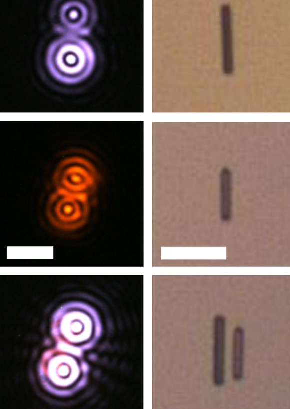
Caption: The researchers also created a multi-wavelength nanolaser system by placing semiconductor nanowires on silicon dioxide. The new transfer printing method could one day allow high-volume manufacturing of chip-based optical systems made of multiple materials.
Credit: Dimitars Jevtics, University of Strathclyde
They also used the printing approach to create semiconductor nanowire lasers by placing nanowires onto host surfaces in spatially dense arrangements. Scanning electronic microscopy measurements of the separation between the nanowires demonstrated a spatial accuracy in the 100-nanometer range. By placing semiconductor nanowires on silicon dioxide, they were able to create a multi-wavelength nanolaser system.
“As a manufacturing technique, this printing approach is not limited to optical devices,” said Jevtics. “We hope that electronics specialists will also see possibilities for how it could be applied in future systems.”
As a next step, the researchers are working to replicate these results with larger numbers of devices to show that it works at larger scales. They also want to combine their transfer printing approach with an automated alignment technique they developed previously to enable rapid measurement, selection and transfer of hundreds of isolated devices for applications in imaging and hybrid optical circuits.
This work was funded by the Engineering and Physical Sciences Research Council (EP/R03480X/1, EP/P013597/1, EP/P013570/1); European Commission (Grant No. 828841 ChipAI-H2020-FETOPEN-2018–2020, Grant No. 829116 SuperPixels -H2020-FETOPEN-2018–2020) and the Royal Academy of Engineering under the Research Chairs and Senior Research Fellowships scheme. Jack Smith’s PhD studentship is co-funded by Fraunhofer UK.
Paper: D. Jevtics, J. A. Smith, J. McPhillimy, B. Guilhabert, P. Hill, C. Klitis, A. Hurtado, M. Sorel, H. H. Tan, C. Jagadish, M. D. Dawson, M. J. Strain, “Spatially dense integration of micron-scale devices from multiple materials on a single chip via transfer-printing,” Opt. Mater. Express 11, 10, 3567-3576 (2021).
DOI: https://doi.org/10.1364/OME.432751.
About Optica Publishing Group
Optica Publishing Group is a division of the society, Optica, Advancing Optics and Photonics Worldwide. It publishes the largest collection of peer-reviewed and most-cited content in optics and photonics, including 18 prestigious journals, the society’s flagship member magazine, and papers and videos from more than 835 conferences. With over 400,000 journal articles, conference papers and videos to search, discover and access, our publications portfolio represents the full range of research in the field from around the globe.
About Optical Materials Express
Optical Materials Express is an open-access journal focusing on the synthesis, processing and characterization of materials for applications in optics and photonics. It is published by Optica Publishing Group and emphasizes advances in novel optical materials, their properties, modeling, synthesis and fabrication techniques; how such materials contribute to novel optical behavior; and how they enable new or improved optical devices. The Editor-in-Chief is Andrea Alù from City University of New York, USA. For more information, visit Optical Materials Express.
Media Contact
